
Research
Integration of optical isolator with laser diode
Integrated optical isolator
High-functioning switching devices
Wavelength-selective Sswitch for on-chip WDM networks
Low-power-consumption magneto-optic switch with self-holding operation
Waveguide magneto-ptical memory
Photonic computing device for AI photonic accelerator
Convolutional neural network with non-volatile optical gate
Photonic Neuron
Visible-light devices with optical waveguides
Planar beam scanner with magneto-optical effect
Photonic integrated circuits
Integration of optical isolator with laser diode
Integration of optical isolator with laser diode
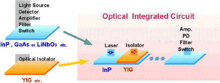
We developed a technology to integrate an optical isolator and a laser diode by wafer direct bonding of magneto-optical crystal with III-V compound semiconductor.
Wafer direct bonding
The direct bonding technique provides the wafer bonding without adhesive. The direct bonding of magnetooptic garnets to III-V compound semiconductors is invesitgated in this research group. It has been demonstrated that (LuNdBi)3(FeAl)5O12 wafers on which optical waveguides are fabricated are bonded onto InP substrates and GaInAsP layer MOCVD-grown on the InP substrate.
_LNB.gif)
Optical isolator integrated with laser diode
An optical isolator protects optical active devices, such as a laser diode and an optical amplifier from unwanted reflected light. This is essential to stabilize the operation of active devices. The novel optical isolator composed of semiconductor waveguide, which is integrable with LD, is investigated. The isolator employs nonreciprocal phase shift in an in-plane magnetized magnetooptic crystal. The magnetooptic crystal like an iron garnet is directly bonded with III-V semiconductor guiding layer by using wafer direct bonding. The features of the device are single polarization operation and easy control of magnetization.
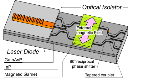
The above figure illustrates the operation of the isolator employing nonreciprocal phase shift. Lightwave launched out from the laser diode passes to the right output port as indicated in red color.
The lightwave reflected back from the external circuit propagates as indicated in blue color, which is not injected into the laser diode.
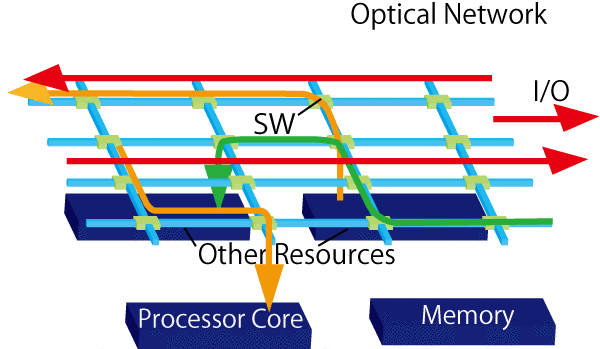
High-functioning switching devices
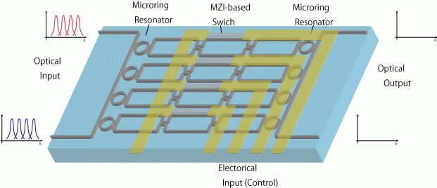
Wavelength-selective switch for on-chip WDM networks
Optical fiber communication is capable of long distance transmission with high capacity using wavelength division multiplexing (WDM) technology. Recently, it is required even in short-distance communiations such as rak-to-rack and board-to-board links. Wavelength-slective switches (WSSs) are typically based on free-space optics employing switching elements such as MEMS and liquid crystal on silicon (LCOS). We have proposed a novel WSS structure based on silicon photonic platform.
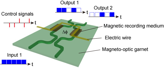
Low-power-consumption magneto-optic switch with self-holding operation
We have proposed a novel self-holding optical switch which holds its switching state without any power supply and consumes power only when the state is changed. This feature is useful for optical cross-connect sysytems or reconfigurable photonic integrated circuits. Magneto-optical (MO) effect in the MO garnet induces phase shift in the interferometer arms. The magnetization of MO garnet is fixed by magnetic field from magnetic-recording medium. Control signals of pulsed current flips the magnetization of the magnetic-recording medium and then changes the optical switching state.
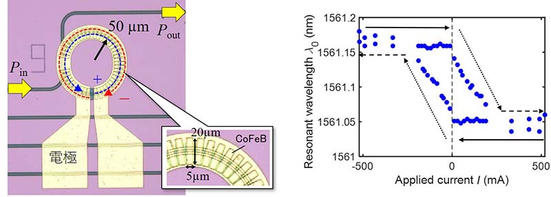
Waveguide magneto-optical memory
We investigate magnetic optical memory that converts optical signal information into magnetic information and stores it in a nonvolatile manner. Magneto-optical recording is achieved using a soft magnetic thin film as a recording layer and magneto-optical garnet as a reading layer. Write light is input while a weak external magnetic field is applied, and magnetization is reversed by weakening the coercive force of the recording layer due to heat generated by light absorption.
Photonic computing device for AI photonic accelerator
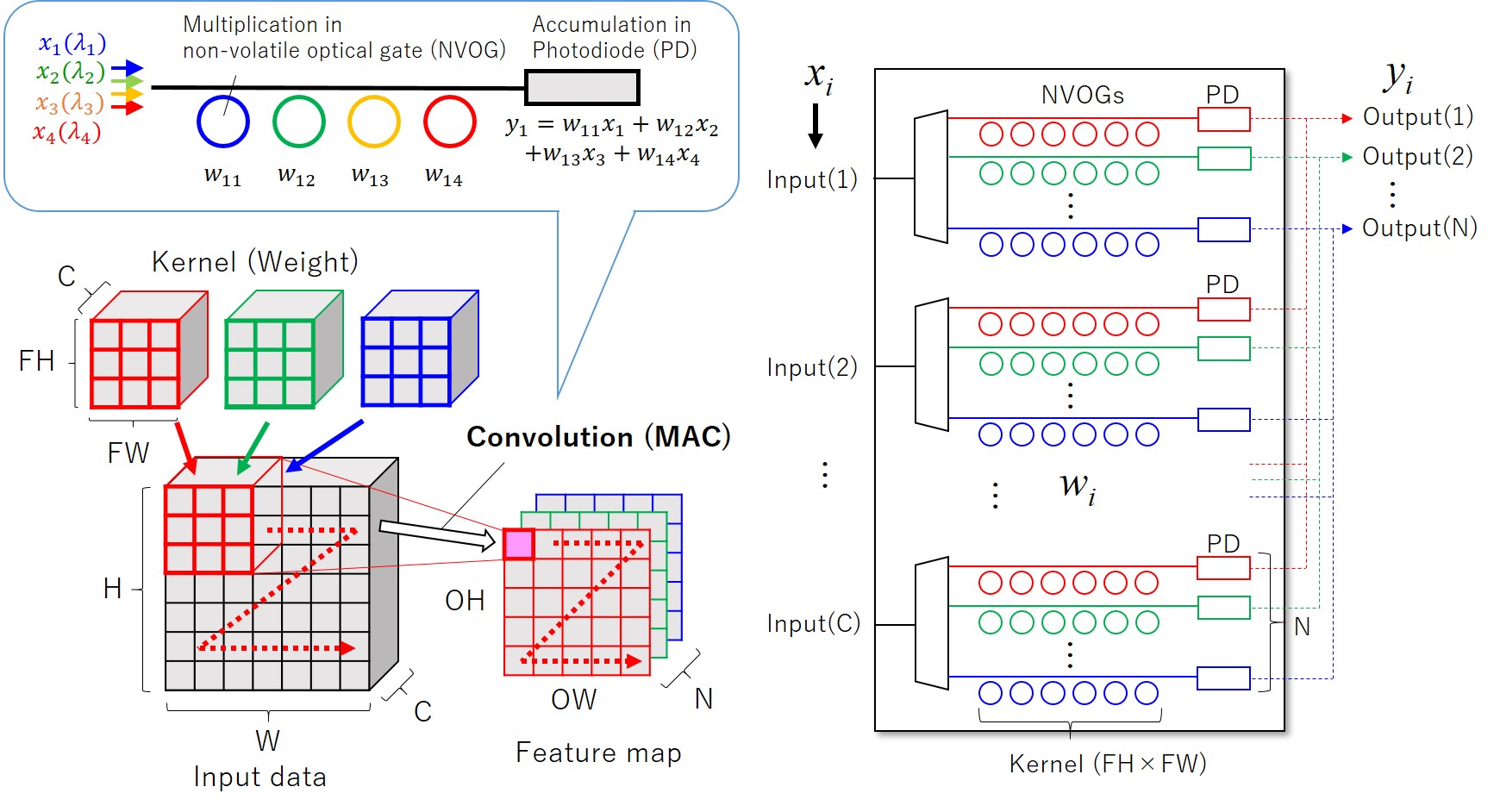
Convolutional neural network with non-volatile optical gate
Artificial intelligence (AI) continues to develop rapidly, and its computational processing capacity is becoming enormous. Dedicated hardware specialized for such calculations is called an "AI accelerator", and photonic AI accelerators with ultra-high capacity and low latency are attracting attention. In this research, we aim to realize a programmable and low-power-consumption optical arithmetic circuit by using non-volatile optical elements that operate by the magneto-optical effect. In particular, we are conducting research to implement the multiple-and-accumulation operation of convolutional neural networks (CNNs), which are known to have a large processing load in deep learning, on photonic integrated circuits.
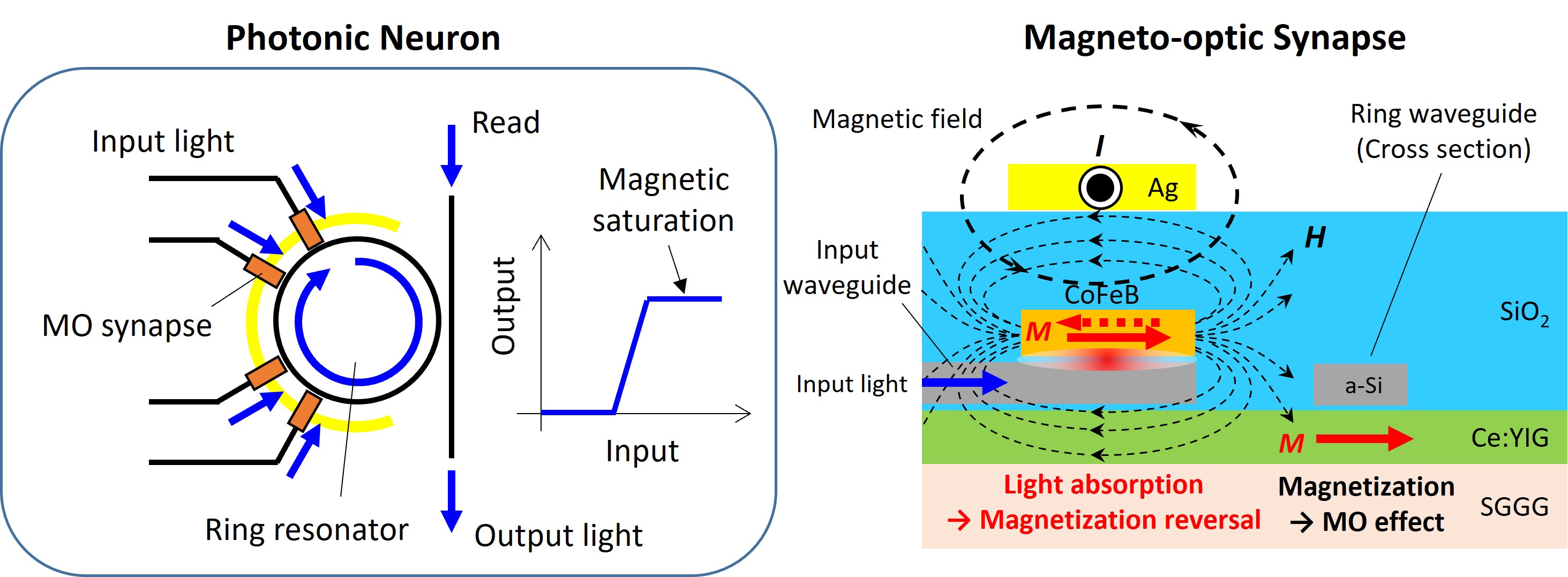
Photonic neuron
An artificial neural network is a method that models the structure of the human brain's neurons and performs calculations, and through repeated learning, it becomes possible to recognize images, sounds, etc. with high precision. Neurons, which are the basic elements, perform complex information processing by repeating signal integration and firing through information transmission. Photonic AI accelerators are physically constructed neural networks using photonic circuits and light signals. In this research, we aim to create artificial neurons that operate with light signals by simulating synapses. With a configuration that closely resembles the structure of actual neurons, it is possible to reproduce the spike firing phenomenon and create an on-chip learning mechanism.
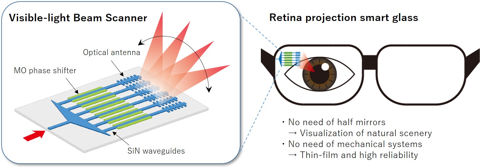
Visible-light devices with optical waveguides
Planar beam scanner with magneto-optical effect
Augmented Reality (AR) is a technology that displays a virtual world superimposed on the real world, and is attracting attention as a next-generation technology that utilizes a variety of information to make people's lives more convenient and enriching. The most important device is the AR display, and in this research we investigate a flat beam scanner using optical waveguide technology with the aim of creating smart glasses that are thinner, lighter, and have better visibility than ever before. By using the magneto-optic effect, it enables faster light modulation compared to liquid crystals.